
OPTO-EDU A63.7190 300000x Microscope điện tử quét kích thước quan trọng
-
Kích thước bánh xốpA63.7190-68: 6/8 inch
-
Nghị quyết2.5nm (Acc=800V)
-
Tăng tốc điện áp0,5-1,6kV
-
Khả năng lặp lạiTĩnh & động ± 1% hoặc 3nm (3 sigma)
-
Đầu dò hiện tại chùm tia3 ~ 30pa
-
Dải đoFOV 0,1 ~ 2.0μm
-
Nguồn gốcTrung Quốc
-
Hàng hiệuCNOEC, OPTO-EDU
-
Chứng nhậnCE, Rohs
-
Số mô hìnhA63.7190
-
Tài liệu
-
Số lượng đặt hàng tối thiểu1 phần trăm
-
Giá bánFOB $1~1000, Depend on Order Quantity
-
chi tiết đóng góiĐóng gói thùng carton, để vận chuyển xuất khẩu
-
Thời gian giao hàng5~20 ngày
-
Điều khoản thanh toánT/T, Công Đoàn Phương Tây, Paypal
-
Khả năng cung cấp5000 chiếc / tháng
OPTO-EDU A63.7190 300000x Microscope điện tử quét kích thước quan trọng
|
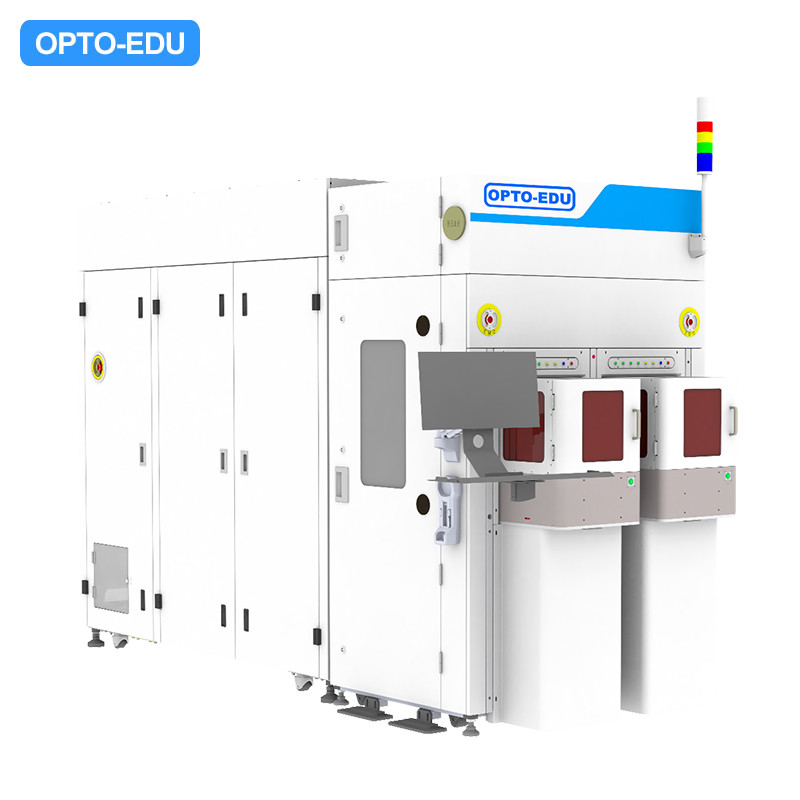
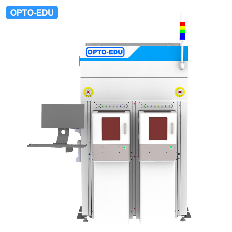
Máy kính hiển vi điện tử quét kích thước quan trọng (CD-SEM) là một SEM chuyên dụng được sử dụng để đo kích thước của các tính năng nhỏ trên các tấm wafer bán dẫn, mặt nạ quang học và các vật liệu khác.Các phép đo này rất quan trọng để đảm bảo độ chính xác và chính xác của các thiết bị điện tử được sản xuất.
️Tương thích với 6/8 inch Wafers kích thước, phóng to 1000x-300000x ️Độ phân giải 2,5nm (Acc=800V), Điện áp tăng tốc 500V-1600V ️Lặp lại Khả năng tĩnh và động ± 1% hoặc 3nm ((3 Sigma), Điện chùm thăm dò 3 ~ 30pA ️Thiết kế hệ thống chuyển wafer tốc độ cao phù hợp với chip bán dẫn thế hệ thứ 3 ️Hệ thống quang điện tử tiên tiến và xử lý hình ảnh, bao gồm máy làm mát, bơm khô |
|
▶Các đặc điểm chính CD-SEM sử dụng chùm electron năng lượng thấp và có hiệu chuẩn phóng đại được nâng cao để đảm bảo đo lường chính xác và lặp lại.và góc bên tường của các mẫu. |
|
▶Mục đích CD-SEM rất cần thiết cho đo lường trong ngành công nghiệp bán dẫn, giúp đo kích thước quan trọng (CD) của các mẫu được tạo ra trong quá trình lithography và khắc.CD đề cập đến kích thước tính năng nhỏ nhất có thể được sản xuất và đo đáng tin cậy trên một wafer. |
|
▶Ứng dụng Các dụng cụ này được sử dụng trong các dây chuyền sản xuất các thiết bị điện tử để đảm bảo độ chính xác kích thước của các lớp và tính năng khác nhau tạo thành một con chip.Họ cũng đóng một vai trò quan trọng trong quá trình phát triển và kiểm soát, giúp xác định và khắc phục mọi vấn đề có thể phát sinh trong quá trình sản xuất.
▶Ý nghĩa Nếu không có CD-SEM, vi điện tử hiện đại sẽ phải vật lộn để đạt được mức độ chính xác và hiệu suất cao mà ngành công nghiệp yêu cầu.Chúng rất cần thiết để đảm bảo độ tin cậy và chức năng của các thiết bị điện tử hiện đại. |
|
▶Công nghệ thay đổi Khi các kỹ thuật lithography tiến bộ và kích thước các tính năng tiếp tục thu hẹp, CD-SEM liên tục phát triển để đáp ứng nhu cầu của ngành công nghiệp.Các công nghệ và tiến bộ mới trong CD-SEM đang được phát triển để giải quyết những thách thức của việc đo lường các mô hình ngày càng phức tạp |
| A63.7190 Máy hiển vi điện tử quét kích thước quan trọng (CDSEM) | ||
| Kích thước wafer | A63.7190-68: 6/8 inch | A63.7190-12: 12 inch |
| Nghị quyết | 2.5nm (Acc=800V) | 1.8nm (Acc-800V) |
| Điện áp tăng tốc | 0.5-1.6KV | 0.3-2.0KV |
| Khả năng lặp lại | Static & Dynamic ± 1% hoặc 3nm ((3 Sigma) | Static & Dynamic ± 1% hoặc 0.3nm ((3 Sigma) |
| Dòng tia thăm dò hiện tại | 3 ~ 30pA | 3 ~ 40pA |
| Phạm vi đo | FOV 0,1 ~ 2,0μm | FOV 0,05 ~ 2,0μm |
| Dữ liệu thông | > 20 miếng/giờ, | > 36 miếng/giờ, |
| 1 điểm / chip, | 1 điểm / chip, | |
| 20 Chips/Wafer | 20 Chips/Wafer | |
| Tăng kích thước | 1Kx ~ 300Kx | 1Kx-500Kx |
| Độ chính xác của giai đoạn | 0.5μm | |
| Nguồn điện tử | Máy phát điện nhiệt Schottky | |
| So sánh các mô hình CDSEM chính trên thị trường | |||||
| Thông số kỹ thuật | Hitachi | Hitachi | Hitachi | Opto-Edu | Opto-Edu |
| S8840 | S9380 | S9380 II | A63.7190-68 | A63.7190-12 | |
| 1. Kích thước wafer | 6 inch/8 inch | 8 inch/12 inch | 8 inch/12 inch | 6 inch/8 inch | 12 inch |
| 2. Nghị quyết | 5nm (Acc=800V) | 2nm (Acc=800V) | 2nm (Acc=800V) | 2.5nm (Acc=800V) | 1.8nm (Acc=800V) |
| 3. Điện áp tăng tốc | 500-1300V | 300-1600V | 300-1600V | 500-1600V | 300-2000V |
| 4. Khả năng lặp lại (chính xác và động) | ± 1% hoặc 5nm ((3 sigma) | ± 1% hoặc 2nm ((3 sigma) | ± 1% hoặc 2nm ((3 sigma) | ± 1% hoặc 3nm ((3 sigma) | ± 1% hoặc 0,3nm ((3 sigma) |
| 5. IP Range (Sonde hiện tại) | 1-16pA | 3-50pA | 3-50pA | 3-30pA | 3-40pA |
| 6. Kích thước FOV | - | 50nm-2um | 0.05-2um | 0.1-2um | 0.05-2um |
| 7.Thông ra | 26 miếng/giờ, | 24 miếng/giờ, | 24 miếng/giờ, | > 20 miếng/giờ, | 36 miếng/giờ, |
| 1 điểm / chip, | 1 điểm / chip, | 1 điểm / chip, | 1 điểm / chip, | 1 điểm / chip, | |
| 5 chip/wafer | 20 chip/wafer | 20 chip/wafer | 20 chip/wafer | 20 chip/wafer | |
Sản phẩm của chúng tôi được bán trên toàn thế giới. Bạn có thể yên tâm về toàn bộ quá trình sản xuất sản phẩm của chúng tôi.